|
No hay comentarios de productos.
DV-505/DVF-4050/-S
CIRCUIT DESCRIPTION
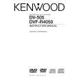
Block Diagram for D/A Converter BCK LRCK DATA Serial Input I/F 8X Oversampling Digital Filter with Function Controller DAC Enhanced Multi-level Delta-Sigma modulator Output Amp and Low-pass Filter Vout L
ML Function MC Control MDI I/F
Vcom
DAC
Output Amp and Low-pass Filter
Vout R
System Clock System Clock Manager ZERO L Zero Detect
SCK
Power Supply
64 Bit SDRAM : HY57V651620B(IC301)
Pin No. 38 37 19 20,21 22~26 29~35 16,17,18 15,39 2,4,5,7,8,10 11,13,42,44 45,47,48,50 1,3,9,14,27 43,49 10 36,40 Pin Name CLK CKE CS BA0,BA1 A0~A11 WE,CAS,RAS LDQM,UDQM DQ0~DQ15 VCC/VCC Q VSS/VSS Q NC I/O I I/O I/O Description The system clock input. all other inputs are registered to the SDRAM on the rising edge of CLK Controls internal clock signal and when deactivated,the SDRAM will be one of the states among power down, suspend or self refresh. Enables or disables all inputs except CLK, CKE, and DQM. Selects bank to be activated during RAS activity. Selects bank to be read/written during CAS activity. Row address : RA0~RA11, Column address : CA0~CA7 Auto-precharge flag : A10 WE, CAS and RAS define the operation. Controls output buffers in read mode and masks input data in write mode.
DGND VCC VDD
ZERO R
Multiplexed data input/output pin. Power supply for internal circuits and input buffers. Ground terminal. Unused.
Flash Memory : M29F400T-90N1(IC401)
Pin No. 25,24~16,8~1 29,31,33,35 38,40,42,44 30,32,34,36 39,41,43 45 26 28 11 12 15 47 37 27,46 Pin Name A0~A18 DQ0~DQ7 DQ8~DQ14 DQ15 CE QE WE RP RY/BY BYTE VCC VSS I/O I I/O I/O I/O o Description Address Inputs Data Input/Outputs, Command Inputs Data Input/Outputs Data Input/Outputs or Address input Chip Enable Output Enable Write Enable Reset/Block Temporary Unprotect Ready/Busy/Output Byte/Word Organization Supply Voltage Ground
8
AGND
|